What's the first thing you do when...
... you get an expensive new toy?You tear it apart of course!
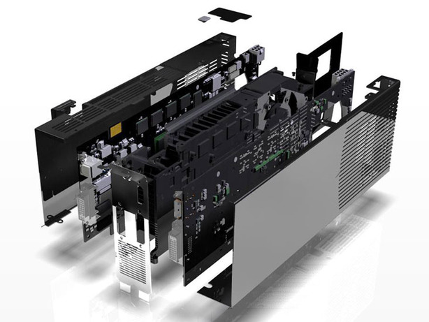
And that's exactly what I did when our first GeForce 9800 GX2 arrived – I simply couldn't resist, even though Nvidia had provided us with an exploded view of the card.
That said, if you're looking to buy a GeForce 9800 GX2, I recommend not taking it apart unless you're planning to watercool it. I say this because it's not only rather difficult to take apart, but probably even harder to put it back together.
This is because the card is fully enclosed inside a metal housing – we'll be covering the external design in due course and before we get distracted, we should really talk about what's under the heatsink!

No GeForce 9800 GX2s were harmed in this explosion...
Nvidia said that the way to get the most out of the two GPUs on the card was to have them on separate PCBs. However, unlike the GeForce 7950 GX2, Nvidia decided that the best way to cool the pair of G92 chips was to sandwich a cooler in between them.
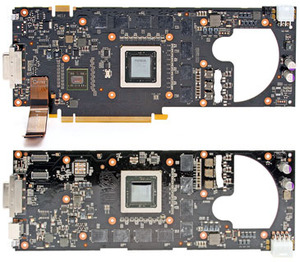
Although the two GPUs sit facing each other when the card is assembled, the second GPU on the PCB without the PCI-Express connector is rotated by 90 degrees. The 'bottom' edge of the GPU facing the display connectors on the end of the PCB – the PCI-Express traces come out of this edge of the GPU and route towards the PCI bracket as well.
Note: from now on, we'll call that PCB2 and we'll refer to the other as PCB1 for simplicity.
The traces go all the way to the two connectors on PCB2 right next to the DVI port and, from here, data is transferred across the two ribbon cables to PCB1. At the other end of the card, there is a three phase power circuit along with several other surface mount components and an eight-pin PCI-Express power connector.
The reason why PCB2 has an eight-pin connector and not a six-pin one is because it doesn't have a PCI-Express interconnect and, if you remember back to our original GeForce 8800 GT review, you'll know that G92 clocked at 600MHz core and 1,500MHz shader will consume around 105W at peak. Even if it's more like 95W on this PCB, that's still 20W more than you can physically draw through a six-pin power connector.
PCB1, on the other hand, features only a six-pin power adapter – this is because it can also draw 75W through the PCI-Express interconnect and the extra components don't count towards a massive difference in power requirements. And despite the differences, there is still a three phase power circuit on this PCB.
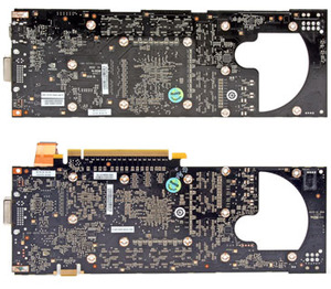
The PCI-Express interconnect doesn't send data directly to the GPU on PCB1; instead, it communicates with the BR04-300 chip – this is a 48-lane PCI-Express 2.0 switch with CPU Broadcast and PW Shortcut functionality (covered on the previous page). Nvidia won't comment on TDP and transistor counts, but it's a small chip that's not going to significantly contribute to the heat produced by the card.

MSI MPG Velox 100R Chassis Review
October 14 2021 | 15:04


Want to comment? Please log in.