
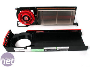
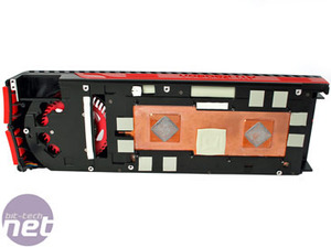
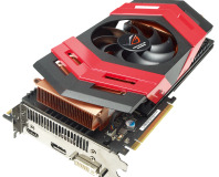
The vapour channel cooler is a one piece component, compared to the HD 4870 X2 which featured two separate coolers
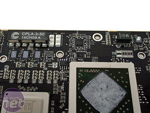
The plastic shroud adds a good inch on after the end of the fan: ATI clearly loves the aesthetic addition, even though it takes the card over the foot long mark! The underside of the heatsink is crafted precisely to cool all the necessary areas of the card, although big thick thermal pads are included to bridge the small gaps. The GPU cores are coated with normal TIM - and there's plenty slapped on there.
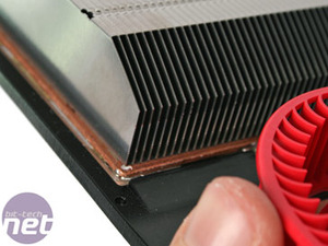
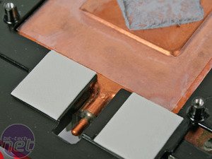
The vapour channel is completely sealed - we can see the nipple where the gas is injected. The aluminium fins are soldered on directly.
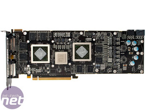
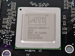
Aside from the two GPUs, the bridge chip is immediately obvious. Despite looking very much like the PLX chip used in the previous HD 4870 X2, this time it's actually ATI branded. It's still fabbed in Taiwan - we assume at TSMC along as with everything else ATI. Its job is the same, too - to split and balance the single PCI-Express 2.0 x16 connector equally between the two GPU. Both of the GPUs are rotated so that their PCI-Express pins face this chip directly.
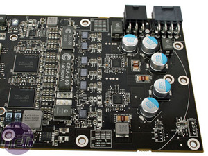
Just as with the Radeon HD 4870 X2, there are three power phases per core, and an additional one for memory. In contrast the 5870 gets a 4+2 arrangement to play with, whereas the 5850 features a 3+2 layout. On the 5970, there are also an additional two phases at the top of the stack near the rear of the card we've yet to attribute to something specific. There's also space for an extra phase on both cores and a second 8-pin connector too - but it looks like it wasn't needed because of the lower core clocks and limited overclocking potential due to temperature limitations. It ATI does fancy releasing a 5980/5990 later on, obviously there's space for growth.

MSI MPG Velox 100R Chassis Review
October 14 2021 | 15:04




Want to comment? Please log in.