
A closer inspection...
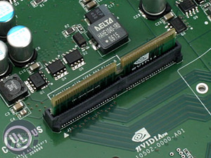
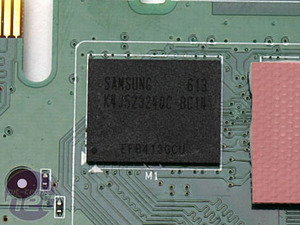
Back when we reviewed GeForce 7900 GX2, we took the time to take the card apart in order to explain how the technology works from a physical perspective. In essence, the GeForce 7950 GX2 uses many of the same principles as the GeForce 7900 GX2, but the implementation is a little more refined in order to get Quad SLI ready for the mass market.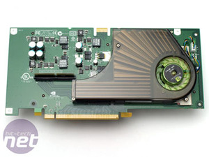
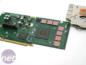

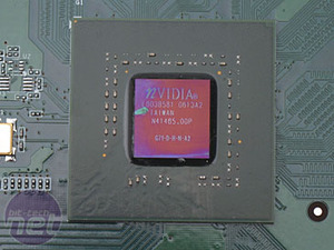
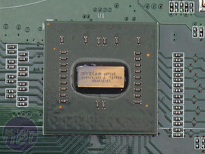
As a result of using a 48-lane PCI-Express switch between the two PCBs, there is a need for a bridge chip in order to make the GPUs work together in tandem. Typically, a pair of GPUs working in SLI mode send data across the SLI bridge connector and PCI-Express bus. Obviously, there is no physical PCI-Express bus between the two GPUs on the GeForce 7950 GX2, so NVIDIA had to make its own using a PCI-Express to PCI-Express bridge chip. This is very similar to the AGP to PCI-Express (and PCI-Express to AGP) bridge chip that we have seen on a number of NVIDIA products where the SKU wasn't using the GPUs' native bus interconnect.

MSI MPG Velox 100R Chassis Review
October 14 2021 | 15:04



Want to comment? Please log in.