Vega’s Architecture
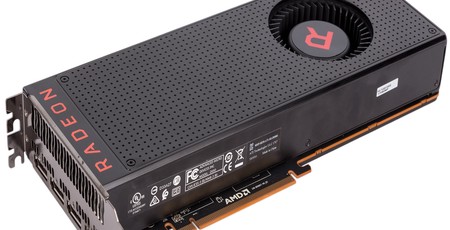
The Vega 10 GPU is built on a 14nm FinFET LPP (low-power plus) process and comprises a whopping 12.5 billion transistors. AMD has not confirmed die size at the time of writing, but we do know that this is AMD's first GPU using this newly tweaked version of its Graphics Core Next (GCN) architecture as well as its largest and most complex design ever. It's also its first GPU to leverage the Infinity Fabric interconnect also utilised by AMD's Zen architecture in its Ryzen and Threadripper CPUs. This interconnect has an independent clock frequency, and AMD plans to leverage it in the future for faster chip development. It will also, of course, play a pivotal role in AMD's upcoming Raven Ridge APUs that combine Zen and Vega cores onto a single chip.
AMD has not supplied a block diagram for Vega 10 as it usually does, but it has summarised the chips layout. Four Asynchronous Compute Engines and one Graphics Engine at the front end feed a pipeline comprising four of the new Next-Gen Geometry Engines and 64 NCUs (which give you the total 4,096 stream processors and 256 texture units). There are 64 Render Back-End units in total, which are now clients of the L2 cache, which has been doubled from its 2MB implementation in Fiji to 4MB here.
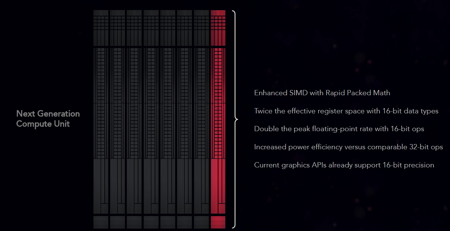
This implementation of GCN brings with it the first major update to AMD's Compute Unite, which is effectively the building block of GCN. While raw IPC hasn't changed, effective IPC has been increased by the introduction of Rapid Packed Math, effectively the ability to handle a pair FP16 (half-precision) instructions in a single FP32 unit, thus potentially doubling throughput per clock cycle in optimal scenarios. A wider instruction set is supported to enable this. AMD says it has implications for lighting, procedural, post-processing, ray tracing, and AI operations, and such operations are already supported in modern APIs.
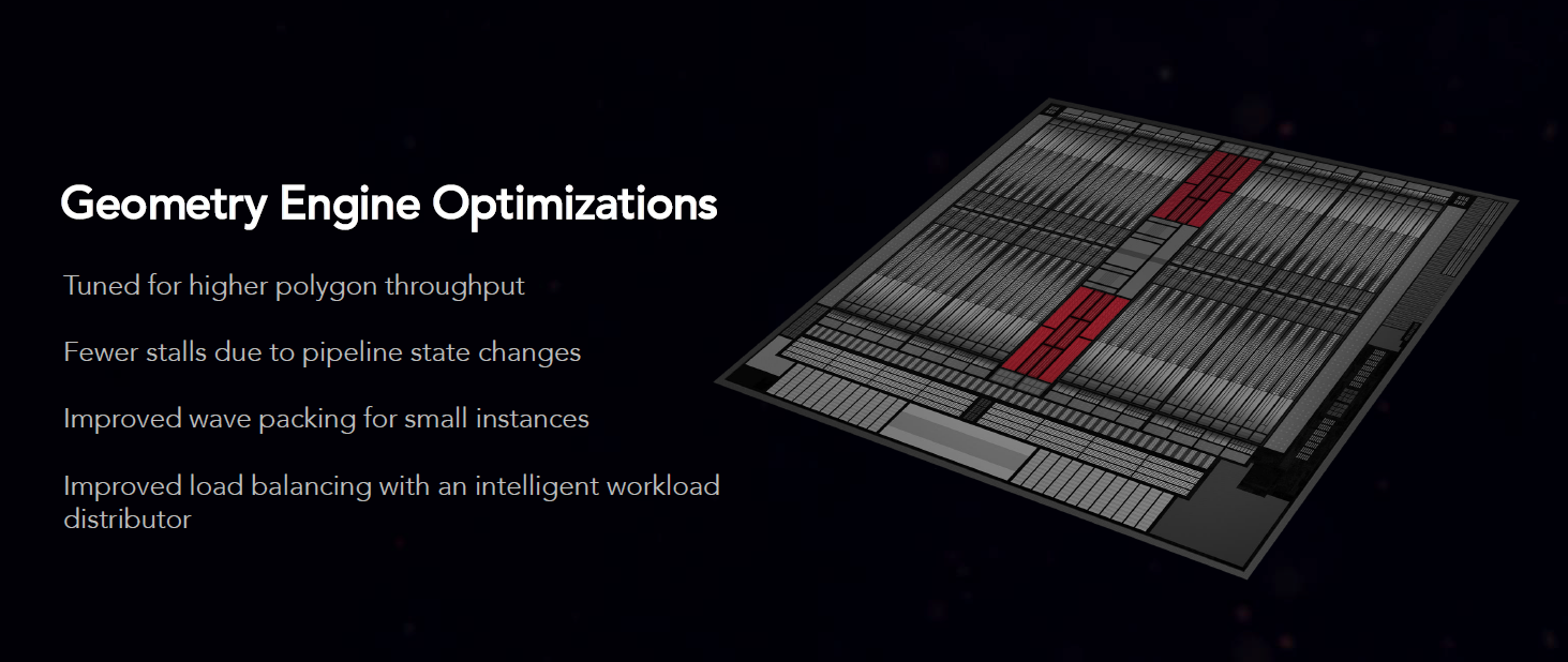
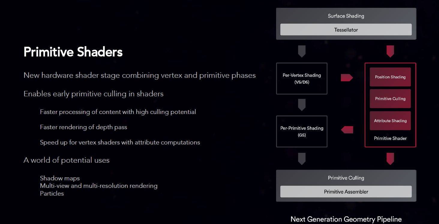
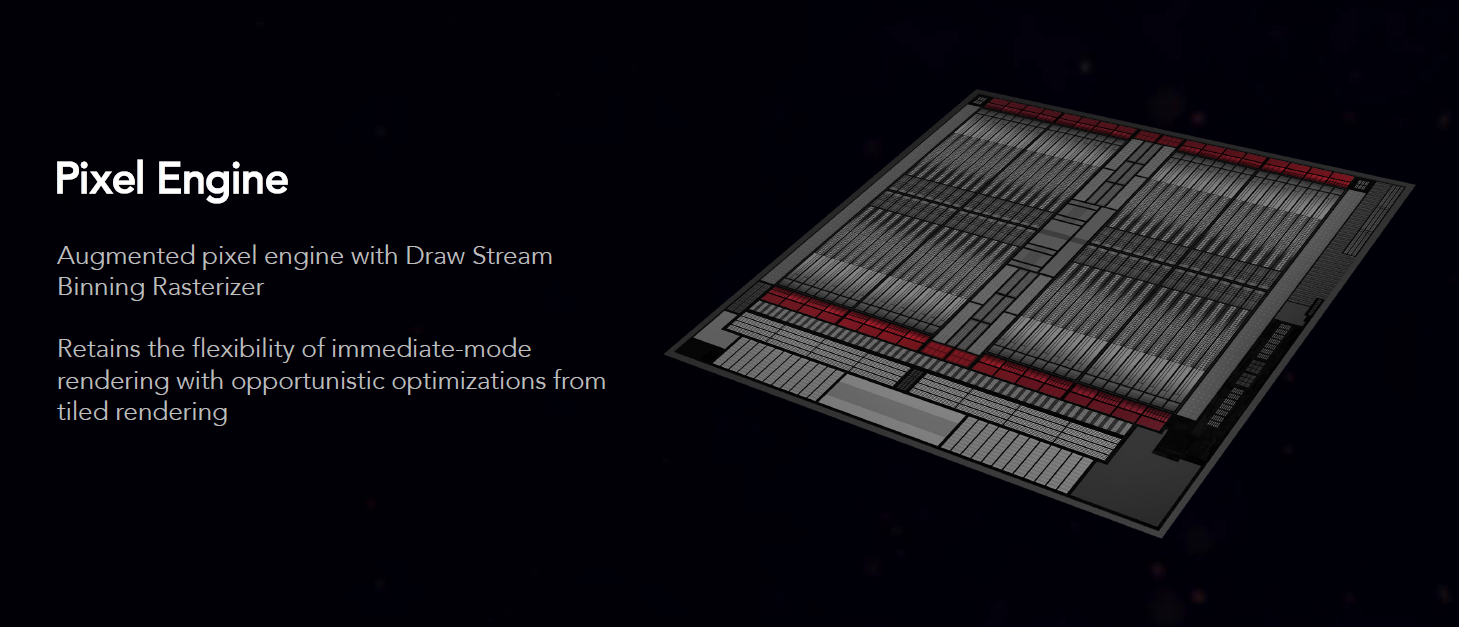
Other pieces of the puzzle include the Next-Generation Geometry Engine, which AMD says allow it to achieve both higher polygon throughput and more efficient load balancing in conjunction with its new Primitive Shaders (a new hardware stage between surface shading and the rasterisation), and the new Pixel Engine which has also been tweaked for efficiency. A few more details regarding these can be seen on the slides on this page.
Something that's always going to boost performance is an increase in raw clock speed, and AMD says it has finely tuned Vega 10 on many fronts to go much faster than before. When building the NCU, for example, it optimised the physical layout by shortening the wire lengths of performance-critical paths, with the end result being a Compute Unit that can go roughly 400MHz faster. Microarchitectural tweaks across the ASIC were also carried out to improve timings, and AMD says that Vega is capable of hitting speeds in excess of 1.7GHz, which compares favourably to Fiji at around 1GHz and Polaris at around 1.3GHz.
Speaking of clock speeds, it's worth noting that AMD is taking a different approach to how it represents them. Previously, it would only list the chip's boost clock in its official specifications, but this represented only the maximum the chip would reach; power, thermal, and noise limits could easily constrain it to lower clocks. Now, AMD is listing a base and a boost clock similar to Nvidia, and they function in the same way. The base clock is the true baseline performance (excluding low-power states), while the boost clock is more akin to the typical or average clock speed you can expect when the GPU is under load, but in the right conditions it can and will boost higher. AMD also promises a broader range of clocks and quicker transitions between them, and it has implemented a new micro-controller for onboard power management.


MSI MPG Velox 100R Chassis Review
October 14 2021 | 15:04




Want to comment? Please log in.