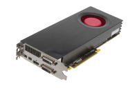
AMD ATI Radeon HD 5770 Review
Manufacturer: AMDUK Price (as reviewed): £119.99 (inc VAT)
US Price (as reviewed): $159.99 (ex Tax)
AMD has been busy of late as it has started to roll out its Radeon HD 5000 'Evergreen' series of graphics cards. We've already looked in depth at the architecture behind the new Evergreen chips - particularly focusing on Cypress - and we've evaluated the gaming experience delivered by the Radeon HD 5870.
For reasons completely out of our control, we haven't said an awful lot about the Radeon HD 5850 yet, but the good news is that there'll finally be a full bit-tech review of that online tomorrow.
Today, AMD is launching the ATI Radeon HD 5700 series with two new graphics cards that sit below the Radeon HD 5850 and 5870 in the performance mainstream segment. We've been told to expect the Radeon HD 5770 to sell for around £120, while the cheaper Radeon HD 5750 will likely sell for about £100.
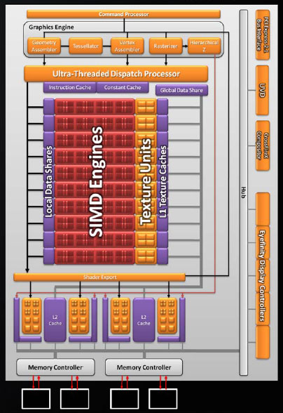
Juniper's Architecture Flow Diagram
The Radeon HD 5770 uses Juniper in its full form with all 10 SIMD cores enabled, clocked at 850MHz - the same frequency as the Radeon HD 5870's engine. Each of these SIMD cores has 16 five-way superscalar shader processors, four texture units, a 32KB local data store and an 8KB L1 texture cache, resulting in a shader core not too dissimilar to the Radeon HD 4870's (RV770).
There are some changes inside, as the shader units learned some new tricks in the Radeon HD 5000 series - we discussed these at great length during our Radeon HD 5870 Architecture Analysis.
The global data store has remained unchanged and still stands at 64KB - AMD still doesn't talk about the bandwidth between local and global data stores. The Graphics Engine hasn't remained exactly the same, as the dual rasteriser and hierarchical-Z units are no longer required - Juniper is half the size of Cypress and it doesn't suffer from the same bottlenecks in this area.
The back end of the chip has also been cut in half, as there are only two 64-bit memory controllers, each with two ROP units that can each handle four colour writes or 16 Z/stencil writes per clock. The Functionally, L2 caches haven't changed from Cypress and there are just half as many of them (two instead of four) - they're still 128KB each and the theoretical peak bandwidth between L1 and L2 still stands at 435GB/sec.
To continue the similarities with the 5870, the 5770 shares the same memory clock too at 1,200MHz (4,800MHz effective), which means it has 76.8GB per second of bandwidth because of its 128-bit memory interface, meaning it has precisely half the memory bandwidth of AMD's current flagship part.
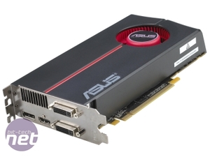
Finally, AMD has modified the display engines slightly. Cypress featured six display output engines arranged in two groups of three (traces for all three engines are required to enable each group); Juniper includes five display output engines - they're still arranged in two groups and only the larger of the two groups is enabled on the Radeon HD 5770 reference card with dual dual-link DVI, HDMI and DisplayPort outputs, meaning the list of supported configurations is the same as it is on Cypress. We asked AMD if there were plans for an EyeFinity Edition, but it would not comment.

MSI MPG Velox 100R Chassis Review
October 14 2021 | 15:04




Want to comment? Please log in.