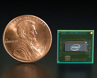
Taiwan Semiconductor Manufacturing Company (TSMC) has announced that its 55nm process technology is ready for use in large scale production.
The new process is a half node based on the company's existing 65nm process and should allow chip designers to shrink their existing 65nm designs to 55nm with a minimal amount of risk and effort.
Because shrinking from 65nm to 55nm is a linear process, die sizes should be reduced by around 15 percent. As a result, both yields and the number of dies per 300mm wafer will increase and, according to TSMC, power consumption should be reduced by around 10 to 20 percent without any reduction in gate switching speed.
The 55nm logic family includes general purpose (GP) and consumer (GC) platforms. Initial production of the 55GP begins this quarter and 55GC production will start later in the year.
Chip designers and IP suppliers will be able to make use of the semiconductor manufacturer's CyberShuttle prototyping programme, which is expected to start using 55nm process technology on a bi-monthly basis from May this year.
I guess this means we can expect the likes of ATI and Nvidia to start testing the new process technology over the next few months. We're unlikely to see products manufactured on the new technology much before the end of the year, though.
Discuss in the forums

MSI MPG Velox 100R Chassis Review
October 14 2021 | 15:04


Want to comment? Please log in.