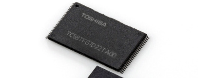
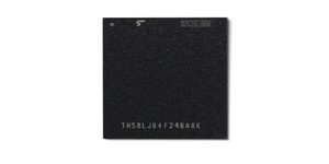
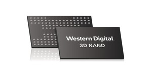
Toshiba and SanDisk have announced the development of the first 48-layer three-dimensional stacked-cell flash memory modules, dubbed BiCS 2, sampling now ahead of mass production next year.
With Moore's Law - the observation by Intel co-founder Gordon Moore that the number of components on an integrated circuit doubles roughly every 18 months - under threat thanks to the growing complexity of shrinking to ever-smaller feature and production node sizes, interest in three-dimensional manufacturing techniques has exploded. Traditional integrated circuits are planar in nature, with all component features laid out on a flat surface in two dimensions. While there have been exceptions, such as Intel's tri-gate transistor and the similar FinFET technologies, this has long been the standard - but new components are appearing which use multiple component layers stacked in three dimensions.
An obvious progression from package-on-package (PoP) layouts, three-dimensional stacked layouts allow for high feature density in a very low footprint without moving to a smaller production node. The production technique is of most interest to memory makers, and Toshiba is working to bring its benefits to flash memory.
BiCS, as Toshiba has christened its new flash module, uses two-bit-per-cell NAND flash components in an array of 48 layers to produce a single module holding 128 gigabits (16GB). As well as boosting capacity per module, the move is claimed by Toshiba to improve write endurance and speed over planar or lower-layer 3D equivalents, and will first appear in solid-state drive applications - including those from SanDisk, which has co-developed the BiCS technology with Toshiba.
'We are very pleased to announce our second generation 3D NAND, which is a 48 layer architecture developed with our partner Toshiba,' claimed Dr. Siva Sivaram, executive vice president for memory technology at SanDisk. 'We utilised our first generation 3D NAND technology as a learning vehicle, enabling us to develop our commercial second generation 3D NAND, which we believe will deliver compelling storage solutions for our customers.'
While Toshiba has indicated that sample shipments are beginning today, the first mass production of the new modules isn't scheduled until mid-2016 when the company's Yokkaichi Operations Fab 2 facility is officially opened.

MSI MPG Velox 100R Chassis Review
October 14 2021 | 15:04


Want to comment? Please log in.