Hybrid Memory Cube performance doubles
February 26, 2014 | 11:06
Companies: #altera #hybrid-memory-cube-consortium #micron

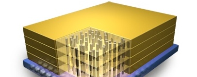
The Hybrid Memory Cube Consortium has announced its second-generation specification, promising to double the throughput of its innovative three-dimensional memory technology.
The Consortium, led by Samsung and Micron and joined in 2012 by Microsoft, has been pushing its HMC technology for some time. Designed to stack memory wafers using through-silicon via technology to create a three-dimensional cube, HMC promises much: the original first-generation designs, which began shipping in September last year, offered a peak transfer rate around ten times greater than the fastest DDR3 memory in a compact footprint and with a power draw some 70 per cent lower than its traditional planar competition.
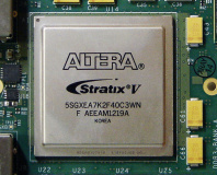
Now, the Consortium has announced the second generation of the HMC specification, which further increases the throughput. According to figures released by Micron, co-founder of the Consortium, the short-reach performance has been boosted from a previous peak of 15Gb/s to 30Gb/s - a doubling which will significantly increase overall performance of the parts. 'The HMC Gen2 specification doubles the interface data rate, which enables system designers to more easily realize performance gains with next-generation 20nm and 14nm FPGAs and SoCs,' explained Patrick Dorsey, senior director of product marketing at HMC Consortium member and FPGA specialsit Altera. 'Our early start in delivering evaluation boards and the demonstrated interoperability between Hybrid Memory Cube devices and FPGAs enables customers to immediately start evaluating and developing HMC-based, high-performance systems.'
Although it will be some time before second-generation parts hit mass production, early adoption of the first-generation Hybrid Memory Cube modules has shown promising gains over planar RAM - leading to the possibility that the technology will trickle down to the desktop in the not-too-distant future.

MSI MPG Velox 100R Chassis Review
October 14 2021 | 15:04


Want to comment? Please log in.