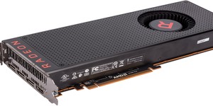
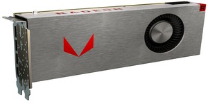
AMD has officially taken the wraps off its next-generation Vega graphics processor architecture, pointing to the improvements it hopes will help it win back market share lost to discrete graphics leader Nvidia.
Vega, due to launch early this year and appearing first in the company's Radeon Instinct accelerator family, is being positioned by the company as being a major leap over previous generation graphics processors. In support of this claim, the company has treated the tech press to a technological overview of just why Vega should have a place in everything from gaming rigs to high-performance computing projects.
The company's promises for Vega begin boldly, with the claim that it includes 'the world's most scalable GPU memory architecture'. Using High Bandwidth Memory 2 (HBM2), the company is claiming a doubled bandwidth per pin and eight-fold capacity increase per stack, along with a halved footprint compared with off-chip GDDR5 memory. A high-bandwidth cache controller linked to system RAM, meanwhile, is claimed to offer smart movement of data between system RAM and video RAM - resulting, the company claims, in lower overall VRAM requirements when running games at Ultra HD resolution.
Vega also includes an entirely refreshed programmable geometry pipeline, offering a claimed doubling of peak throughput per clock, which combines nicely with what the company describes as an 'Intelligent Workgroup Distributor' for improved load-balancing between the processor's various components and pipelines.
The meat of Vega, though, comes in what the company calls its 'Next-Generation Compute Unit', or NCU. This, the company claims, offers 512 8-bit, 256 16-bit, or 128 32-bit floating-point operations per clock and can be split for high-performance, mixed-precision mathematics. The chip is also optimised for both higher clock speeds and increased number of instructions per clock (IPC), packing up to four operations where the company's previous compute units would have managed only one.
Additional improvements promised in the Vega architecture include a draw stream binning rasteriser, which is claimed to both boost performance and reduce power draw, while the shifting of render back-ends to act as clients of the level two (L2) cache boost the performance of deferred shading.
There's one thing that didn't form part of AMD's presentation, however: real world figures. While the company has crowed about the potential improvements available from Vega as a result of its architectural changes, it has not yet put its money where its mouth is and subjected Vega-based cards to real-world benchmarking. AMD has also yet to formally confirm launch dates and card specifications for Vega's release.

MSI MPG Velox 100R Chassis Review
October 14 2021 | 15:04


Want to comment? Please log in.