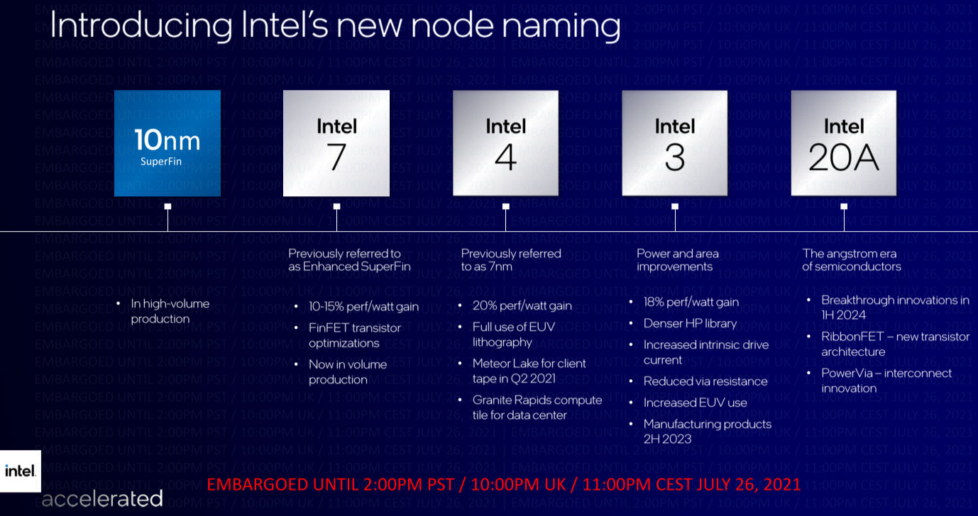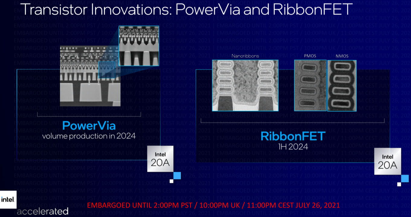
An Intel Accelerated webcast went live on Monday, with a number of important announcements. The hour-long live-streamed event outlined Intel's plans to switch-up its node naming strategy to be more meaningful, and make it appear to be more in step with the likes of TSMC and Samsung. Additionally, Intel shared information about two breakthrough technologies dubbed RibbonFET and PowerVia, and it talked about its expanded/optimised Foveros 3D stacking technologies. Lastly, it welcomed big hitters Qualcomm and Amazon AWS as Intel Foundry Services (IFS) customers.

Above, you can see the new node naming scheme from Intel. The next generation consumer desktop and laptop CPUs from Intel, the Alder Lake processor family, won't be known as Intel Enhanced 10nm SuperFin chips when they launch later this year – instead they will be the first 'Intel 7' processors (as will Sapphire Rapids data centre CPUs).
Explaining the change, Intel says that the new scheme will "give customers a more accurate view of process nodes across the industry," and this is all the more important now that IFS has been established. It backed up its claims of the new naming scheme being better / more appropriate with quotes from journals like Semiconductor Engineering and IEEE Spectrum. TSMC's VP of corporate research, Philip Wong was quoted too, saying "Today these numbers are just numbers. They're like models in a car… it's just a designation for the next technology node… So let's not confuse the name of the node with what the technology actually offers". TSMC prefers to use its 'Nx' naming scheme, rather than use nanometers.

Moving along Intel's roadmap, you can see that to the far right, the 'Angstrom Era' starts with Intel 20A in approx H1 2024. This also ushers in some important technologies. RibbonFET, Intel's implementation of a gate-all-around transistor, will be the company's first new transistor architecture since it pioneered FinFET in 2011. Intel says this design "delivers faster transistor switching speeds while achieving the same drive current as multiple fins in a smaller footprint". PowerVia will debut at Intel 20A too. Intel says that PowerVia uses chip through via channels to deliver power from the rear of the chip, eliminating power routing from the front side of the wafer.
A year or so after Intel 20A, we should expect Intel 18A, which is already in development for early 2025. It will debut refinements to RibbonFET for a "major jump in transistor performance". Intel is working closely with ASML on other 'beyond EUV' tech, too.
On the topic of complementary tech, Intel is continuing to refine and optimise its 3D chip packaging. It will advance Foveros 3D stacking tech with; Foveros Omni for mixing multiple top die tiles with multiple base tiles across mixed fab nodes, and Foveros Direct which "moves to direct copper-to-copper bonding for low-resistance interconnects and blurs the boundary between where the wafer ends and where the package begins," according to the chipmaker.
Intel also took the time to provide updates on its business progression since IDM 2.0 and IFS was announced. It appears to have already lined up two big customers for its services; Qualcomm for SoC production using Intel 20A, and Amazon AWS for IFS packaging solutions.

MSI MPG Velox 100R Chassis Review
October 14 2021 | 15:04


Want to comment? Please log in.