IBM declares 1.8nm transistor tech breakthrough
October 5, 2015 | 11:30
Companies: #ibm #intel #research #researchers

IBM researchers have made a breakthrough in transistor engineering which could see Moore's Law continue its trend-line for a few more years yet - and, unsurprisingly, it involves carbon nanotubes.
IBM has been playing with nanotechnology and interesting carbon creations for years, recently unveiling a 9nm carbon nanotube transistor with a plan to commercialise the technology by the early 2020s. Now the company is claiming that it has completed the groundwork required to take transistor technology well below the 9nm mark, following up its ]7nm process node technologies with a roadmap pointing the way to 1.8nm - a fraction the size of today's commercial 28nm to 10nm parts.
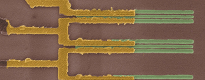
The breakthrough comes from a means of reducing the contact resistance of the carbon nanotube transistors as the feature size - and therefore contact surface area - decreases. The research, carried out at IBM's Thomas J. Watson Research Centre in New York and published in the latest issue of the journal Science, saw the contact resistance greatly reduced at small feature sizes through the use of molybdenum films. The result: projections that suggest that the contact resistance would remain usably low at feature sizes as low as 1.8 nanometres.
The research is part of the semiconductor industry's continued efforts to adhere to Moore's Law, an observation turned golden rule by Intel co-founder Gordon Moore that the number of transistors on new processors tends to double roughly every 18 months. To do so, manufacturers have to continually shrink their feature sizes, creating ever-smaller transistors to be crammed into chips that remain roughly the same size - but at sub-10nm process nodes the laws of physics start to get in the way. Even while still in double-figures, node shrinking isn't a straightforward process: Intel recently announced that its 10nm Cannonlake parts would be delayed, after a similar issue with its 14nm parts back in 2013.

MSI MPG Velox 100R Chassis Review
October 14 2021 | 15:04


Want to comment? Please log in.